
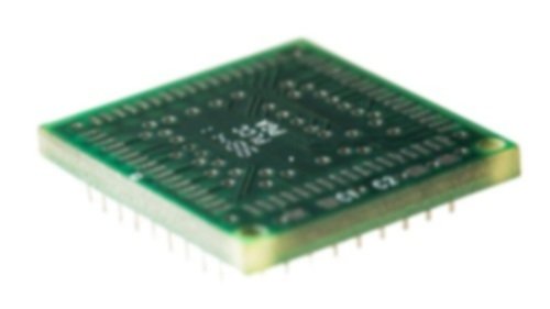
PCB Manufacturing
Murrietta Circuits continues to evolve with the technology demands of our customers. Our custom-built 50,000 sq. ft. PCB manufacturing facility is geared to handle the most complex circuit board requirements, equipped with automated machinery to handle high layer count, thin core, HDI, flex and rigid-flex technologies. Each new product design is thoroughly analyzed through our Genesis DFM software to ensure manufacturability before starting the job.
-
Our manufacturing capabilities span from 2 to 30 layers, providing versatile solutions for a wide range of PCB designs, from basic to complex multi-layered circuitry.
-
We specialize in incorporating blind and buried vias in PCB designs, enabling more compact and efficient circuit layouts.
-
Our manufacturing expertise extends to flexible and rigid-flex PCBs, providing solutions for applications that demand adaptability and resilience.
-
Our manufacturing services encompass a variety of materials including FR4, Polyimide, Lead-Free FR4, Teflon, Ceramic, and High Speed / Low Loss materials, tailored to meet specific project requirements.
-
Leveraging HDI, we integrate advanced interconnect technology into PCB manufacturing, facilitating high-density and high-performance designs.
-
We conduct comprehensive impedance analysis to ensure signal integrity and consistency in our PCB designs, meeting stringent performance requirements.
-
Utilizing top-tier materials from renowned manufacturers such as Isola, Arlon, Ventec, Rogers, Panasonic, and Dupont, we ensure superior quality and performance in our PCBs.
-
We specialize in integrating micro vias in PCBs, enabling greater circuit density and miniaturization without compromising quality.
-
From initial prototypes to full-scale production, we offer seamless and reliable services at every stage of PCB manufacturing.
-
Committed to environmental standards, we adhere to RoHS compliance, providing lead-free PCB manufacturing solutions.
-
Our capabilities include both conductive and non-conductive via filling, ensuring integrity and reliability in PCB designs.
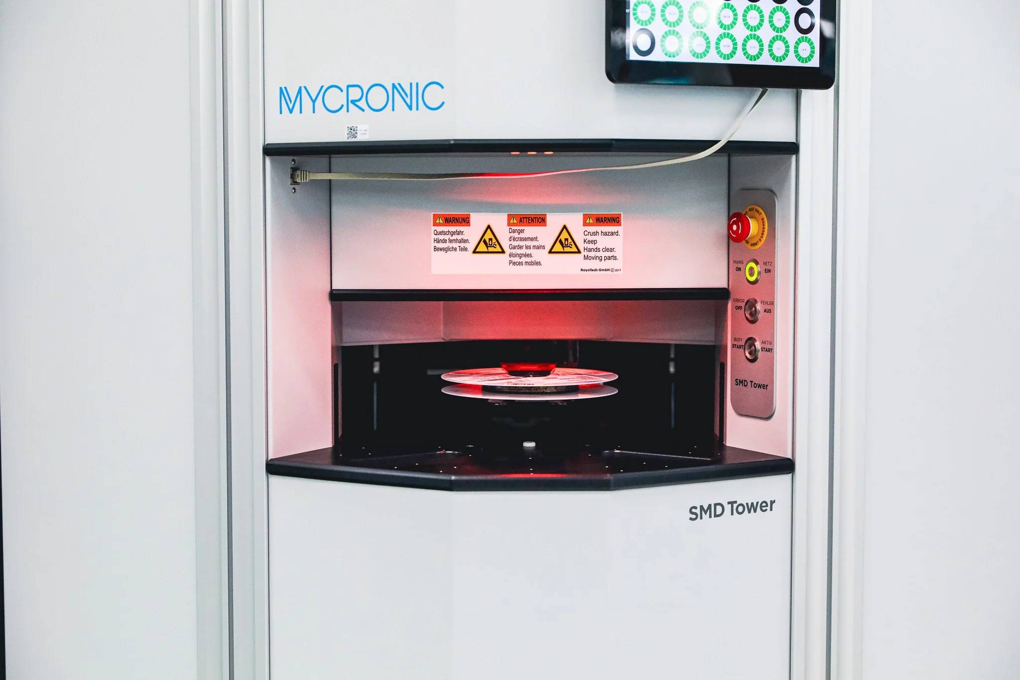
Key Equipment
-
Our investment in a state-of-the-art 4-opening TMP Vacuum Press with high-temperature capabilities ensures precise lamination and pressing for multi-layer PCBs, meeting the most stringent industry standards.
-
Utilizing the Chemcut XLI Alkaline Etch and Tin Strip Line, we ensure precise etching and tin stripping processes.
-
The Chemcut XLI-30 Cupric Etch DES Line, equipped with thin core transport capabilities, ensures accurate and efficient cupric etching processes..
-
Our CIMS Galaxy 25um AOI (Automated Optical Inspection) System employs cutting-edge technology for high-precision, 25-micron accuracy in inspecting PCBs, ensuring adherence to specifications.
-
Employing advanced Copper Pulse Plating Tanks, we ensure precise and controlled copper plating, meeting exacting standards for conductivity and durability in PCB manufacturing.
-
Our Orbotech 8800 Laser Direct Imager utilizes innovative laser technology for precise imaging and etching processes.
-
The Schmoll MX-1 Drill/Router, integrated with a high-resolution camera system, specializes in micro via drilling.
-
Utilizing the advanced Orbotech Genesis CAM (Computer-Aided Manufacturing) Software, we optimize the design-to-manufacturing process.
Relevant Certifications
-
Military performance specification for Printed Circuit Board/Printed Wiring Board, General Specification.
-
Space & Military Avionics Applications Addendum
-
Qualification & Performance Specification for Flexible/Rigid-Flexible Printed Boards.
Other Services
-

PCB Design & Engineering
-

PCB Assembly
-
Component Procurement & Kitting
-
Interposers & Adapters
